Materials Science & Engineering Center
Clean Room Laboratory
Clean Room Zone
Clean Room Laboratory The cleanroom is located in rooms with ISO 5 and ISO 6 cleanliness classes in accordance with ISO 14644.
We provide cleanroom space with a total area of approximately>600 m². 2. In the laboratory, we have continuous monitoring of parameters such as temperature and humidity. Periodic cleanliness measurements confirm the required cleanliness class.
The amount of dust or other microparticles is kept at a constantly low level. Additional rooms intended for lithography are equipped with special lighting systems that minimize the amount of light that could disturb the photolithography process. These conditions enable the production of miniaturized semiconductor and photonic devices, such as microchips.
The laboratory is equipped with advanced infrastructure enabling the complete execution of most stages necessary to fabricate chips: from forming thin layers, through their patterning, to measurement of their properties.
Research techniques
A key piece of equipment used for integrated circuit fabrication is the lithography system: the system for mask alignment for photolithography and the optical maskless lithography system, which enables patterning with a resolution of 1 μm. Lithographic transfer to subsequent layers is possible thanks to wet processes (two reactors for ICP-RIE etching), dry etching, nanoimprinting, and the lift-off technique.
Numerous methods for depositing thin films are also available: from spin-coating soft materials (photoresists, sol-gels) to advanced vacuum techniques such as magnetron sputtering, PE-CVD, and atomic layer deposition (ALD), used for creating metallic and dielectric thin films.
Laboratorium posiada pełną zdolność do analizy i walidacji wytworzonych struktur i warstw, zarówno za pomocą precyzyjnej mikroskopii jak i elipsometrii spektroskopowej oraz dwóch profilometrów – stykowego i optycznego. Cennym uzupełnieniem infrastruktury jest drukarka XTPL umożliwiająca nanoszenie metalicznych linii w skali mikrometrycznej.
Scope and Activities
We provide research services for companies and scientific institutions that require advanced microfabrication techniques and characterization of micro- and nanostructures and thin films. We invite collaboration both in the form of commercial contracts and research collaborations, as well as joint projects. Our team works with many research groups both at PORT and at other institutions, in areas such as III–V semiconductor-based optoelectronics, photonic components based on SiO layers,
2-TiO2 produced using the sol-gel method, as well as advanced materials such as perovskites and artificial opals. We specialize in the fabrication of planar photonic components
photonic using lithographic methods. Our current main research focus is the development of biosensors based on integrated photonic circuits (PICs).
Team members

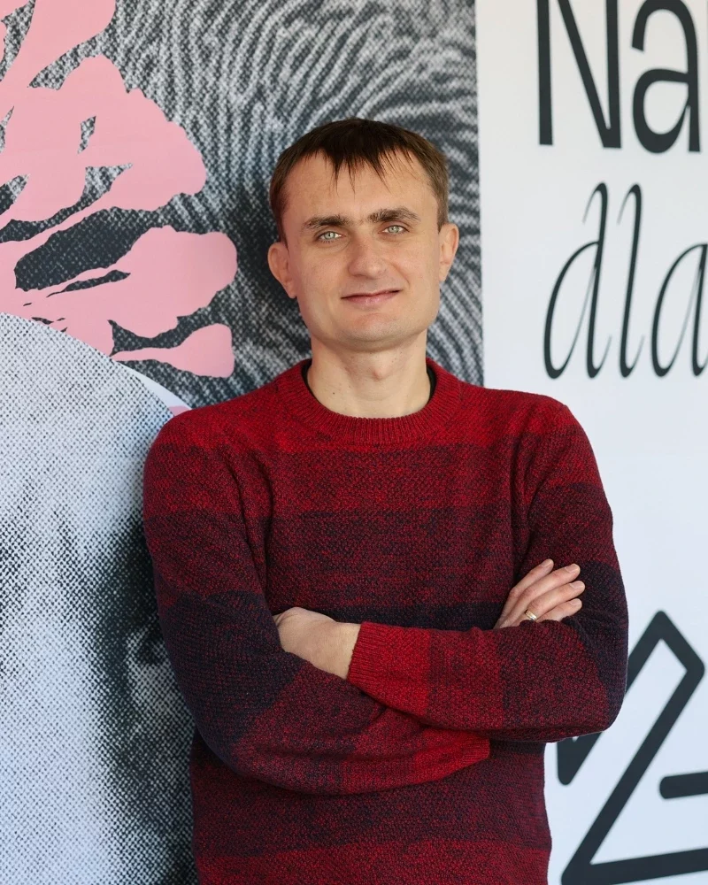
Krzysztof Rola, PhD
He graduated with a master’s degree (2009) in Electronics and Telecommunications, specializing in Microsystem Electronics, from the Faculty of Microsystem Electronics and Photonics at Wrocław University of Science and Technology, where in 2015 he also obtained a doctoral degree in technical sciences in the field of electronics. In his doctoral work, he focused on anisotropic etching of silicon microstructures for applications in MEMS and MOEMS systems.
In 2015–2017, he worked as a specialist at the Institute of Low Temperature and Structural Research of the Polish Academy of Sciences, where he analyzed various materials using electron microscopy (SEM/TEM/EDS). Since 2017, he has been associated with Łukasiewicz – PORT Polish Center for Technology Development (formerly: Wrocław Research Center EIT+), where he has conducted research on photonic crystal and semiconductor technologies. From 2024, he has been responsible for managing the Clean Room Laboratory.
In 2015, he received the START scholarship from the Foundation for Polish Science. He has participated in the implementation of several research projects funded by NCN, FNP, and NCBR. He has co-authored 34 scientific publications cited 331 times (according to Web of Science) and two patent applications; his Hirsch index is 11.
His scientific interests include micro- and nanostructuring using electron microscopy and microfabrication of integrated photonic circuits with potential applications in biosensors. He has extensive laboratory experience in cleanroom work with experimental techniques such as SEM/FIB/EDS microscopy, electron beam lithography, optical lithography, reactive ion etching (RIE), wet etching, thin-film deposition, and ellipsometry.

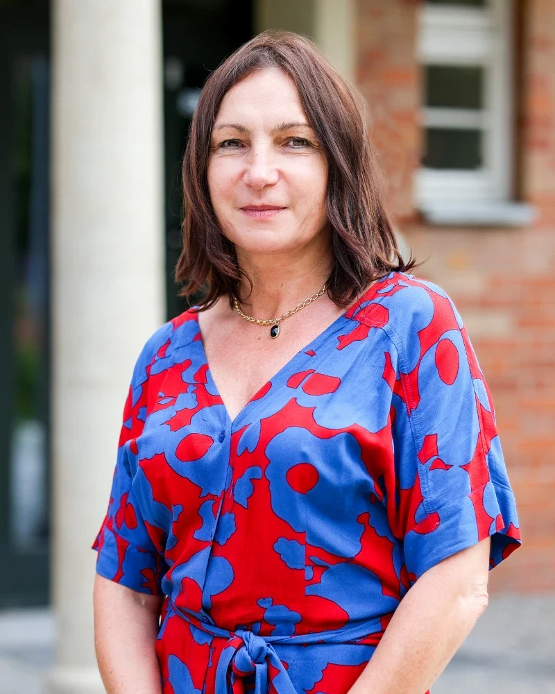
Edyta Piskorska-Hommel, PhD
Since 2017, she has been working at the Łukasiewicz – PORT Polish Center for Technology Development. She conducts research on the fabrication of semiconductor materials using molecular beam epitaxy (MBE). She is also involved in studies of the local structure and electronic structure of functional materials using X-ray spectroscopy methods (XAFS, XANES, EXAFS) with synchrotron radiation. Her research interests include epitaxial semiconductors, catalysts, metal–organic frameworks (MOFs), and materials with a high degree of disorder.
She gained her scientific experience at institutions including the Institute of Physics of the Polish Academy of Sciences in Warsaw, the Institute of Low Temperature and Structure Research PAS, and the University of Bremen (Germany), where she carried out research on the structure of nanomaterials under a DFG fellowship.

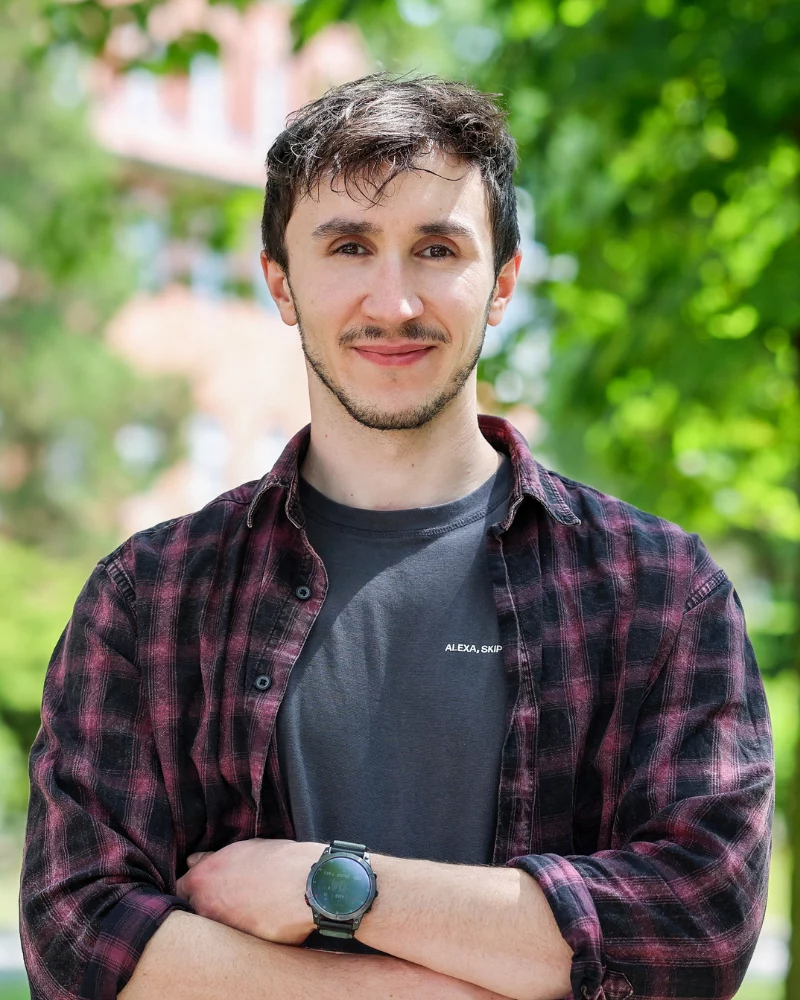
Łukasz Duda, PhD
His scientific activity focuses on the fabrication, structuring and study of liquid-crystalline, polymer and sol-gel materials (including those doped with selected organic dyes). His research is conducted with a view to the potential application of these materials in planar photonics, luminescent sensors, humidity-resistant coatings and biosensors.
At the beginning of his career, Łukasz Duda gained experience in the fabrication and investigation of the properties of mixed liquid-crystalline systems doped with ionic species and systems of hydrogen-bonded molecules. Later, during his industrial doctorate (Doctoral School of Chemistry, Wrocław University of Science and Technology), he gained extensive experience in the fabrication and structuring of thin luminescent films (polymer and sol-gel) of various types on different substrates. In his work he uses a wide range of measurement techniques tailored to a given type of material, enabling comprehensive characterization, including (among others) spectroscopic analysis (UV-Vis and IR range), thin-film surface analysis and the determination of optical properties such as complex refractive index.
Currently, Łukasz Duda focuses on the structuring of thin-film waveguide layers based on SiO₂ and TiO₂ precursors (using soft and hard lithography techniques) as well as their functionalization. His goal is to develop reproducible technological processes for fabricating photonic structures such as Mach–Zehnder interferometers or ring resonators, modified for selected light frequency ranges, which in future may be used to produce integrated biosensors. He also works on fabricating polymer films doped with organic dyes for applications in laser marking using the DLIP method (Direct Laser Interference Lithography).