As part of our website, we use cookies to provide you with the highest level of service, including services tailored to your individual needs. By continuing to use the website without changing your cookie settings, you agree to the placement of cookies on your device as described in our Privacy Policy. You can change your cookie settings in your web browser at any time. Acceptance of essential cookies is required for the proper functioning of the website. For more detailed information, please refer to our PRIVACY POLICY.
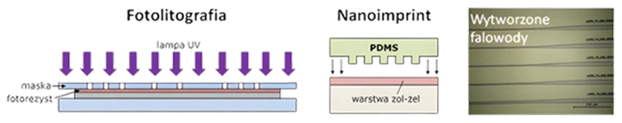
Fabrication of planar photonic components using photolithography, etching, and nanoimprint. Precise photonic components can be fabricated using sequential photolithography and dry etching (RIE) of thin SiO₂–TiO₂ layers. On the other hand, photolithography and/or electron beam lithography are used to fabricate PDMS stamps for nanoimprint. Fabrication of photonic components using PDMS stamps can be a low-cost alternative to other methods of producing integrated photonic circuits.
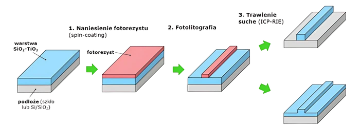
Photolithography enables the fabrication of microscale planar patterns in photoresist layers using photolithographic masks and UV light. Structures formed through photolithography are transferred to subsequent layers using wet or dry etching (Fig. 1) to produce planar photonic components such as waveguides, microring resonators, couplers, interferometers, etc.
These components are fabricated in SiO₂–TiO₂ layers previously prepared using the sol–gel technique. Due to the need to obtain an appropriate refractive index contrast to achieve light guiding, SiO₂–TiO₂ microstructures must be fabricated on glass substrates or Si/SiO₂ substrates.
Fig. 1. Schematic of SiO₂–TiO₂ waveguide fabrication using photolithography and etching.
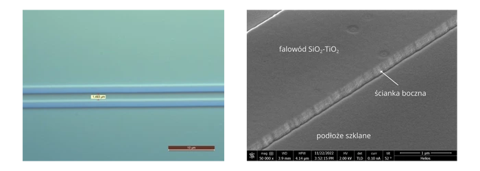
Research on the fabrication of components based on SiO₂–TiO₂ materials focuses on optimization of individual process steps to achieve high structuring resolution and low surface roughness of the etched waveguides.
The resolution of photolithography achieved so far makes it possible to obtain waveguides and ring resonators characterized by a spacing of approx. 1500 nm (Fig. 2a). On the other hand, the process of fabricating waveguides using RIE etching is being optimized with regard to reducing the sidewall roughness of the waveguides (Fig. 2b).
Fig. 2. Photolithography and RIE etching: (left) optical microscope image showing the gap (1500 nm) between the waveguide and the microring resonator, (right) SEM image (52° tilted view) of the waveguide.
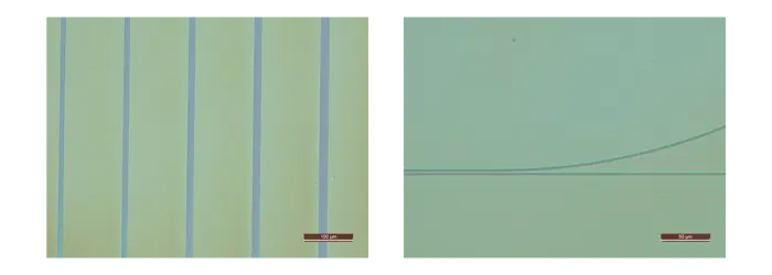
Nanoimprint is the subject of research due to the low cost of fabricating planar photonic components using this technique. This method allows multiple (depending on the degree of process optimization) replications of a pattern from the same previously structured substrate. Waveguides, microring resonators, and other components are first fabricated using photolithography and then replicated in PDMS, from which the resulting molds can serve as stamps for the nanoimprint method in sol–gel materials based on silicon and titanium oxides.
Similarly, more precise and smaller patterns, such as diffraction gratings, are fabricated using electron beam lithography and subsequently replicated in PDMS for the nanoimprint technique. Within the project, the nanoimprint method is being optimized with regard to: appropriate replication depth in sol–gel layers, reduction of layer cracking caused by high-temperature annealing, achieving high resolution, uniformity, and reproducibility of photonic component shapes (Fig. 3).
Fig. 3. Optical microscope image showing SiO₂–TiO₂-based photonic components fabricated using the nanoimprint technique: (left) waveguides of various widths, (right) waveguide and microring resonator.