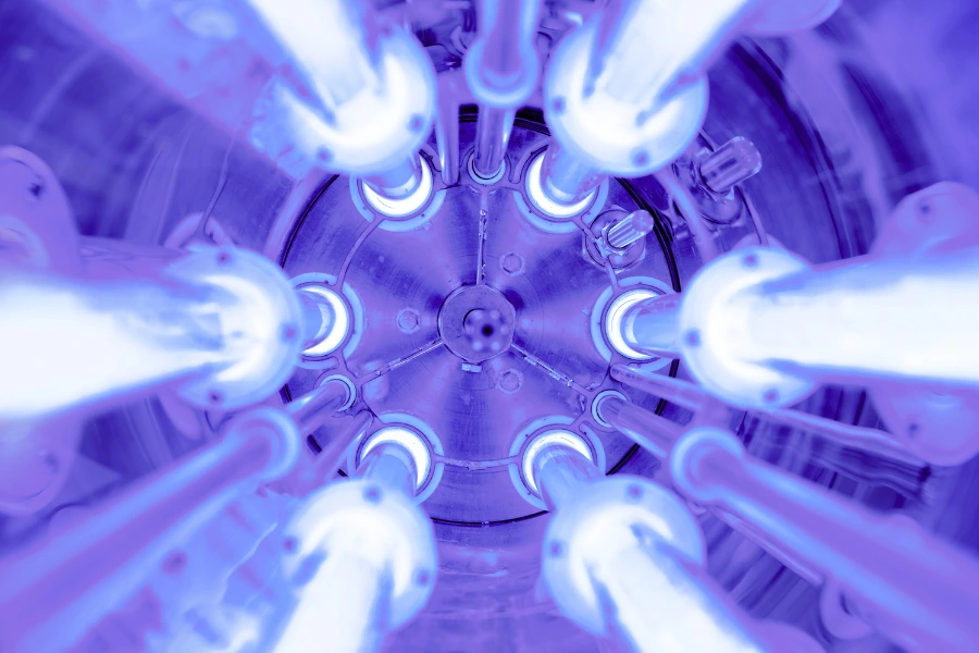
Radiation in the deep ultraviolet (UV-C) range has a unique ability to inactivate bacteria and viruses, making it essential for disinfection and sterilization—from water purification and medical-equipment sterilization to air-sanitization systems in buildings. Demand for fast and safe methods of eliminating biological threats is steadily increasing, and the deep-UV emitter market is expanding rapidly. Analysts estimate that the UV-lamp market will grow by USD 3.25 billion between 2023 and 2027.
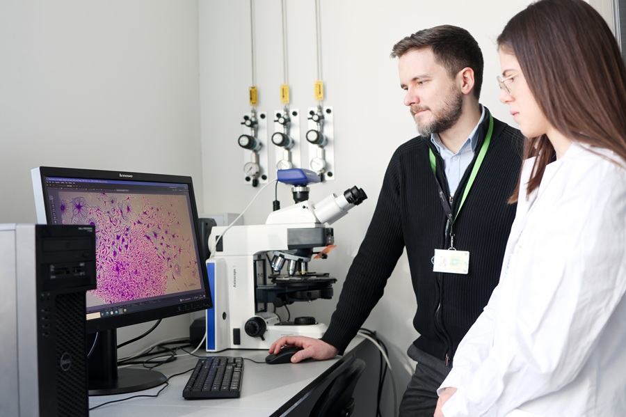
“At the right wavelength—most effectively between 250–270 nm—UV radiation begins to kill bacteria and viruses. That is why deep UV is so important in practice,” explains Dr. Dominika Majchrzak from the Advanced Semiconductor Epitaxy Research Group, a researcher exploring an alternative to traditional deep-UV emitters.
Toward DUV LEDs
Until recently, the most widely used source of UV-C radiation has been mercury lamps. While effective, they have major drawbacks: large size, short lifespan, and the presence of toxic mercury harmful to people and the environment. The scientific community is therefore actively searching for alternatives.
One promising solution is semiconductor DUV LEDs, based on nitride materials (AlGaN). These LEDs are compact, non-toxic, energy-efficient, and durable. However, their efficiency in generating deep-UV light remains low.
“Most of the electrical energy supplied to the LED is converted into heat instead of light. For this reason, LEDs emitting deep ultraviolet currently perform worse than traditional mercury lamps,” explains Dr. Majchrzak.
A major challenge lies in producing high-quality semiconductor layers. LEDs contain two key layers: n-type (electron-conducting) and p-type (hole-conducting). When electrons and holes meet, light is emitted. The most difficult part is the p-type layer, which is notoriously hard to connect efficiently with a metal electrode. Poor electrical contact leads to energy loss and overheating.
“What we need is an ohmic contact—a connection that allows current to flow freely without additional losses. Metals like gold or nickel do not perform well here because their work function is too low. This makes current conduction inefficient and causes a portion of the energy to dissipate as heat rather than light,” says Dr. Majchrzak.
An Innovative Idea: MXenes
A breakthrough idea emerged during a scientific conference where Dr. Majchrzak learned about MXenes—a new class of two-dimensional materials.
“I thought: why not try using them in DUV LEDs? They have metallic conductivity, a high work function, and are easy to deposit. These are ideal properties for electrodes,” she recalls.
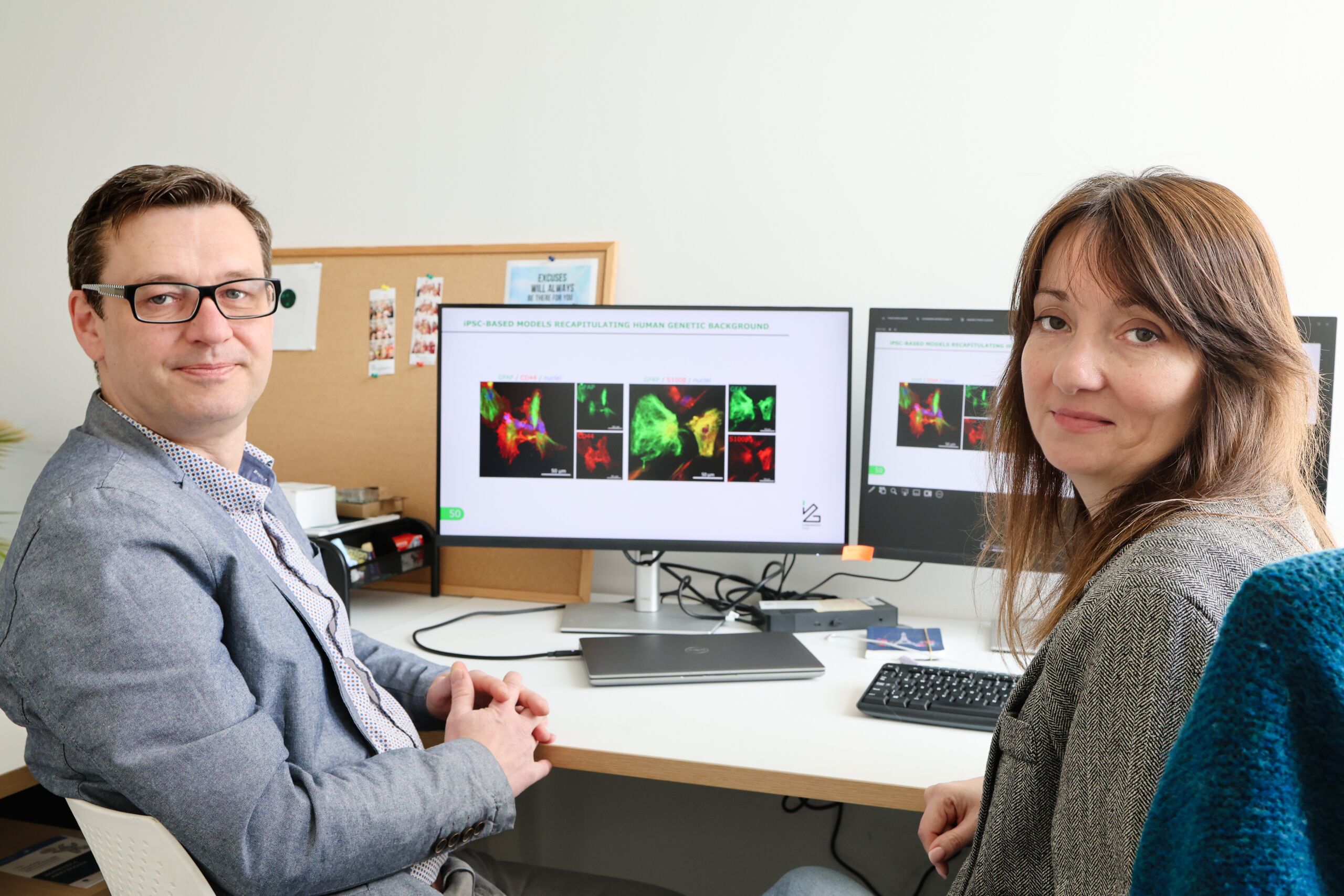
Her project examines whether MXenes can replace conventional metallic electrodes in DUV LEDs. If successful, the LEDs would emit more light and operate longer. Early experimental results from Dr. Majchrzak’s team are highly promising.
Research Internship with a Nobel Laureate
Her project—“Surface Functionalization of p-(Al)GaN Using MXenes: Contact Engineering for High-Efficiency Deep-UV Emitters”—received recognition in the SONATINA 9 competition of the National Science Centre, aimed at early-career researchers. The grant will allow her to continue this work as a postdoctoral fellow and undertake a research internship in California.
At the University of California, Santa Barbara, she will work in the laboratory of Prof. Shuji Nakamura, one of the three Nobel Prize laureates recognized for developing efficient blue LEDs that revolutionized lighting technologies and dramatically reduced global energy consumption. Dr. Majchrzak will gain access to top-tier expertise and cutting-edge equipment.
The Semiconductor Era
Dr. Majchrzak’s research is already attracting interest from technology companies. Her grant proposal received reviews from seven experts, highlighting the strong scientific and industrial interest in the idea. Work on MXenes may help make deep-UV semiconductor emitters more efficient, cost-effective, and accessible.
Semiconductors are frequently in the global spotlight due to rapidly growing demand. They are critical to the development of modern technologies, and recent disruptions in the supply of integrated circuits have shown how essential they are for economic stability and national security.
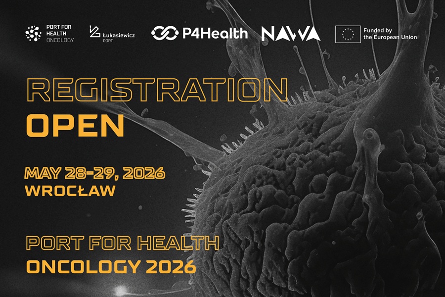
On September 21–24, Wrocław will host an important international discussion on semiconductors. The 8th International Workshop on Ultra-Wide Bandgap Materials and Devices, co-organized by Łukasiewicz – PORT and Wrocław University of Science and Technology, will gather leading researchers in the field. Among the attendees will be Hiroshi Amano, one of the three Japanese scientists—along with Shuji Nakamura and Isamu Akasaki—awarded the Nobel Prize in Physics for the development of blue LEDs.
Wrocław will welcome scientists shaping technological breakthroughs as they explore solutions for current market needs and define the technologies of the future.