Advanced Semiconductor Epitaxy Research Group
The research group focuses on developing novel deep-ultraviolet (DUV) emitters based on group-III nitrides (AlGaInN) in systems featuring unique material combinations that include arsenic, boron, and, in the future, other group-III elements. The group conducts fundamental research aimed at innovative applications in water purification and disinfection technologies for the medical and healthcare sectors. Its work involves studying the use of various epitaxial growth techniques to produce unique multilayer systems.
The main challenges addressed by the group concern the growth of high-quality aluminum-rich structures that meet the stringent requirements of efficient deep-UV light sources.
Group members
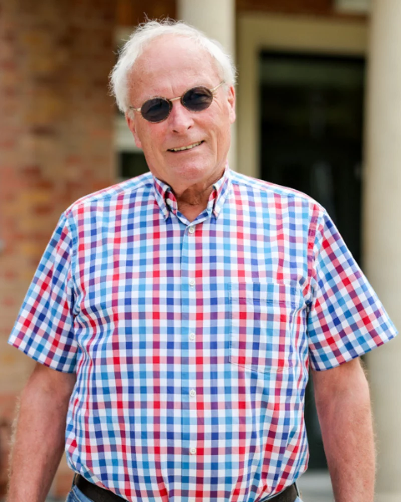
Prof. Detlef Hommel
Prof. Dr. habil. Detlef Hommel received his MSc in Physics from the University of Warsaw in 1975 and his PhD from the same faculty in 1980. He obtained his first habilitation from Humboldt University in Berlin in 1989 and a second one from the University of Leipzig in 1991. In 1993, he was awarded the academic title of Privatdozent at the University of Würzburg. From 1994, he held a full professorship at the University of Bremen. In 2014, he was appointed Professor at the University of Wrocław, and in 2016 he received the title of Full Professor conferred by the President of the Republic of Poland. He is currently the Head of the Advanced Semiconductor Epitaxy Group at Łukasiewicz – PORT.
Prof. Hommel’s scientific interests include condensed matter physics, in particular semiconductors and optoelectronic devices. He specializes in semiconductor epitaxy technologies, nanoscience (quantum dots, nanorods), spectroscopy of rare-earth ions, and heterostructure characterization. His research focuses on wide bandgap materials such as group-III nitrides and II-VI chalcogenides, with applications in single-photon sources and laser diodes.
He is the author of over 700 peer-reviewed publications in renowned journals, including Nature, Nature Physics, Physical Review Letters, Applied Physics Letters, and Nanotechnology. He has led numerous research projects funded by DFG, BMBF, the Volkswagen Foundation, Helmholtz-Gemeinschaft, and national agencies, with a total budget exceeding €8 million. He is the author or co-author of 11 patents related to semiconductor devices, including ZnSe-based laser diodes, p-GaN contact designs, and InGaN quantum dots.
He has supervised over 30 PhD theses and more than 45 MSc theses. He has been invited as a lecturer at universities in Germany, Japan, the USA, and Poland, and has delivered courses in German, English, and Polish.
A member of the Academia Europaea since 2014, Prof. Hommel has served as organizer and chair of numerous international scientific conferences, including the International Workshop on Blue Lasers, E-MRS, and the International Conference on Nitride Semiconductors. From 2003 to 2009, he was the speaker of the DFG Research Group Physics of nitride-based, nanostructured, light-emitting devices. He received an honorary research fellowship from the Alexander von Humboldt Foundation (2006–2009), and has served on several scientific boards, including the Institute of Low Temperature and Structure Research PAS (INTiBS) and the High Pressure Research Institute PAS (since 2024). His research collaborations include UC Santa Barbara, KAUST, CNRS Grenoble, the University of Warsaw, and the Institute of Physics PAS.
He built the Semiconductor Epitaxy Laboratory at the University of Bremen from the ground up, equipping it with dual MBE systems, XPS, FIB, AFM, CAIBE, and advanced instrumentation for electrical and optical measurements. Since 2019, he has served as Chairman of the PORT Foundation. He has also been a member of the Innovation Commission of the Polish-German Chamber of Industry and Commerce and of the KRASP Commission on Large Research Infrastructure.
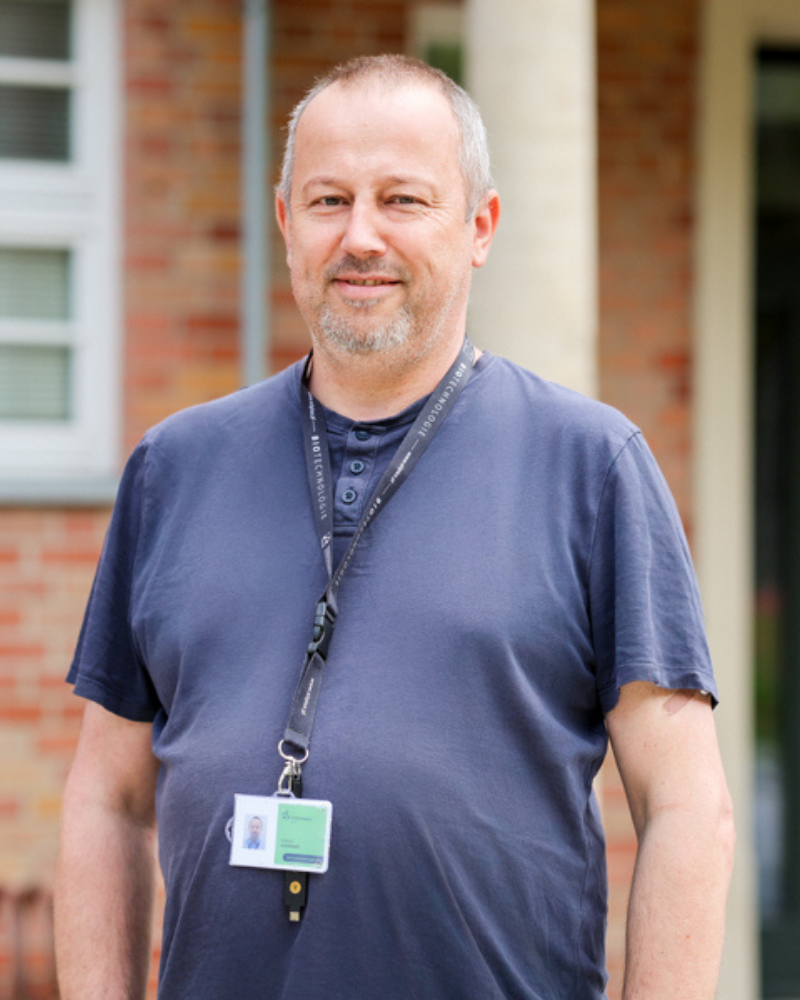
Prof. Robert Kudrawiec
Graduate of the Faculty of Fundamental Problems of Technology at the Wrocław University of Science and Technology, specializing in solid-state physics. Career milestones: MSc Eng. (2000), PhD (2004), habilitation (2010), professor (2018). International appointments: post-doc at Stanford University (Feb 2006–May 2007) and sabbatical at Lawrence Berkeley National Laboratory (Jan 2012–Sep 2013).
Affiliated with PORT since October 2017, currently leading the EpiMat Research Group. He specializes in optical semiconductors and their applications in semiconductor devices, including group III–V (with group-III nitrides), group IV, II–VI, and recently van der Waals crystals and perovskites. Within the HYPHa project, he works on van der Waals crystals and their integration with silica-based waveguides.
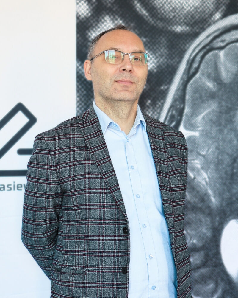
Prof. Jarosław Serafińczuk
Jarosław is a graduate of the former Faculty of Electronics at Wrocław University of Science and Technology, where he completed his master’s studies in Electronics and Telecommunications, specializing in Optoelectronics and Fiber Optic Technology. He obtained his PhD in technical sciences in 2002 at the Faculty of Microsystem Electronics and Photonics of Wrocław University of Science and Technology. In 2018, he received his habilitation degree in the discipline of electronics, and later the title of professor of engineering and technical sciences in the fields of materials engineering as well as automation, electronics, electrical engineering, and space technologies.
He currently works in the Department of Nanometrology at the Faculty of Electronics, Photonics and Microsystems (W12), WUST.
His research focuses mainly on X-ray diffraction in materials studies, particularly high-resolution X-ray diffraction (HRXRD) for analyzing epitaxial structures. He also studies two-dimensional materials and perovskites. His work employs X-ray diffraction and other measurement techniques such as atomic force microscopy (AFM), including the characterization of electrical and mechanical properties.
Prof. Serafińczuk is a co-author of over 100 scientific publications, has developed new research and measurement techniques, supervised two completed PhD theses (and currently supervises two more), and mentored 39 theses. He has led three National Science Centre (NCN) projects (Opus, Sonata, Iuventus Plus) and participated in 21 research projects.
He is a DAAD fellow and participant in prestigious programs such as “Master” (Foundation for Polish Science) and “Young Staff” (WUST).
In 2018 and 2024 he held research stays at the Institute of Nanostructure Technologies and Analytics (INA), University of Kassel. In teaching, he leads courses in nanotechnology, nanodiagnostics, and programming.
Member of the Polish Crystallographic Association.
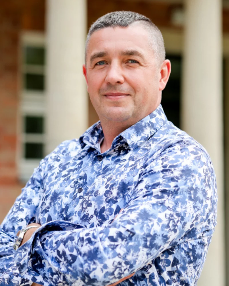
Dr. hab. Damian Pucicki
Damian is employed as a university professor at Wrocław University of Science and Technology, at the Faculty of Electronics, Photonics and Microsystems, in the Department of Nanometrology. At the same time, he serves as a senior research and technical engineer and the head of the Epitaxy Laboratory at Łukasiewicz Research Network – PORT Polish Center for Technology Development in Wrocław. His scientific interests focus primarily on optimizing epitaxial growth conditions (using MOVPE or MBE techniques) to obtain high-quality crystalline layers and semiconductor structures for optoelectronic and microelectronic devices such as transistors, photodetectors, photovoltaic cells, and lasers.
He is also actively involved in the optical and structural characterization of semiconductor heterostructures, which is a key element in optimizing epitaxy conditions and identifying compositional inhomogeneities.
He further specializes in rapid thermal annealing (RTA) processes to reduce structural defects in semiconductor layers, improving their emission, electrical, and crystalline properties. His work also includes developing technological procedures to verify the effectiveness of optimization techniques in epitaxial processes and device structures.
His competencies also include optoelectronic device design optimization, especially quantum well design and electronic structure engineering tailored to device type. Beyond theoretical work, he actively participates in fabrication and characterization of optoelectronic devices, linking fundamental research with applied technologies.
His engineering skills are essential for managing, operating, and maintaining research infrastructure—both in the epitaxy laboratory and across the cleanroom at Łukasiewicz – PORT. He effectively leads a team of scientists and PhD students, acting as a mentor and supervising their epitaxy-related research projects.

Dr. hab. Miłosz Grodzicki
Miłosz is a physicist specializing in experimental surface physics, photoelectron spectroscopy, and solid-state physics. His research focuses on the electronic structure of materials, including semiconductors, two-dimensional (2D) materials, and transition-metal compounds, with particular emphasis on X-ray (XPS) and ultraviolet (UPS) photoelectron spectroscopy conducted under ultra-high vacuum (UHV) conditions.
A physicist specializing in experimental surface science, photoelectron spectroscopy, and solid-state physics. His research focuses on the electronic structure of semiconductors, 2D materials, and transition-metal compounds, with particular emphasis on XPS and UPS in ultra-high vacuum (UHV).
At the Łukasiewicz – PORT, he focuses on group-III nitride semiconductor materials.
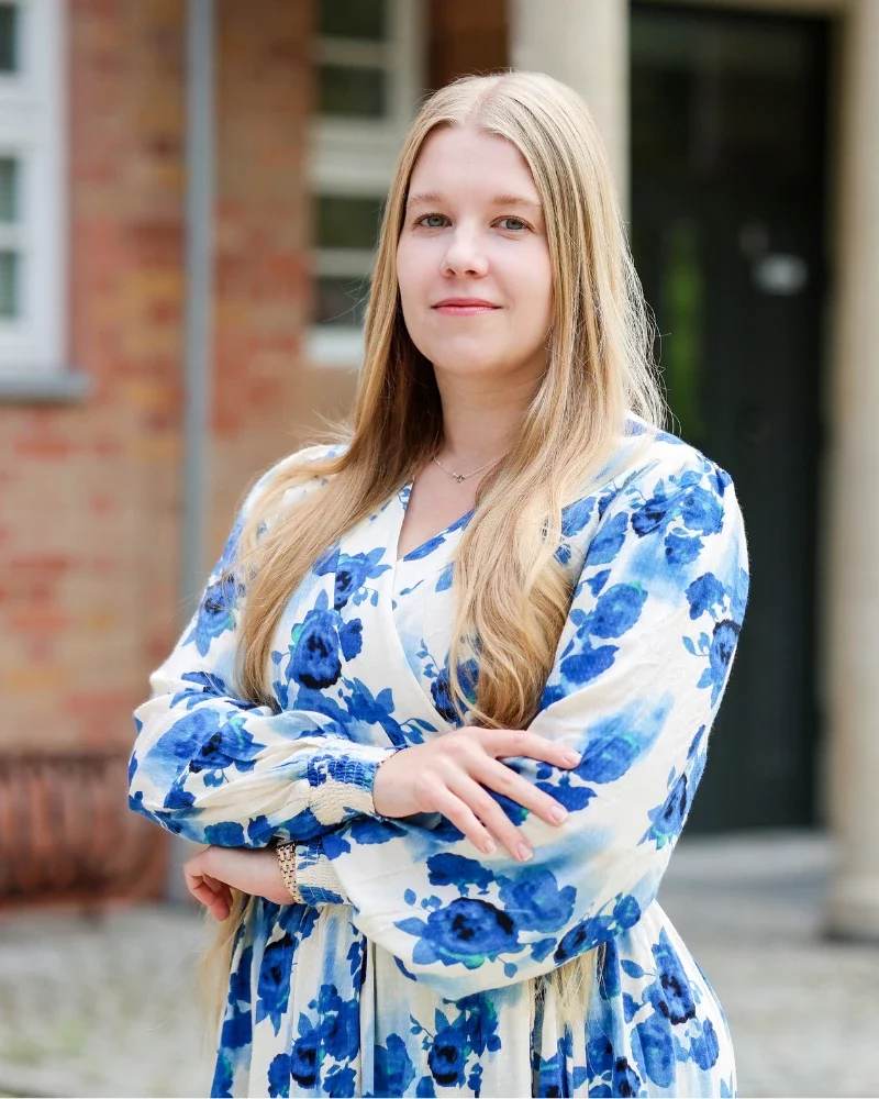
Dr. Paulina Ciechanowicz
Paulina earned a BEng in Nanotechnology and an MSc in Electronics and Telecommunications at the Wrocław University of Science and Technology. She received her PhD from the University of Wrocław, conducting her doctoral research at the Łukasiewicz Research Network – PORT. Her dissertation explored arsenic use in MBE growth of GaN to modify material properties and control growth mode.
This research led to a new arsenic-induced VLS growth method for dodecahedral GaN microwires. The approach is being further developed and optimized within the Semiconductor Compound Epitaxy Research Group. During her PhD, she led an NCN PRELUDIUM project titled “Arsenic-induced VLS growth of dodecahedral GaN microwires by MBE.”
She currently works as a post-doc in the NCN Sonata BIS project “Nitride-based microcolumn UV emitters,” led by Łukasz Janicki, PhD. In the team she specializes in epitaxy of GaN-based microstructures, focusing on GaN microwire structures for LED applications.
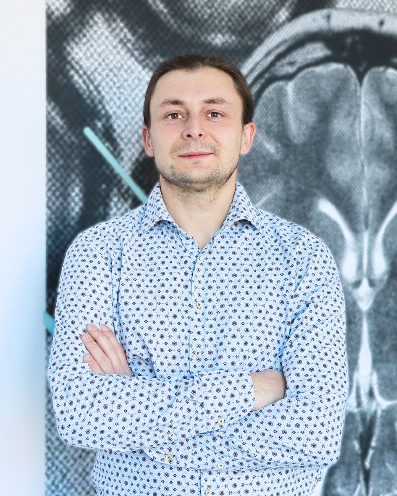
Dr. Łukasz Janicki
Łukasz received his MSc in Physics at the Wrocław University of Science and Technology, where he also completed his PhD. His research focused on group-III nitride materials and structures, with particular emphasis on surface properties analyzed using optical spectroscopy. He performed measurements on bare surfaces and protected surfaces under varied environmental conditions.
For his research, he developed new tools enabling non-contact electroreflectance (and other modulation spectroscopy techniques) at variable temperatures and atmospheric compositions. These results led to his PhD in Physics (2015).
At the Łukasiewicz Research Network – PORT, he works on MBE growth of group-III nitride semiconductor structures, with particular emphasis on microcolumn structures. He leads the NCN Sonata BIS grant “Microcolumn UV emitters based on nitrides.”
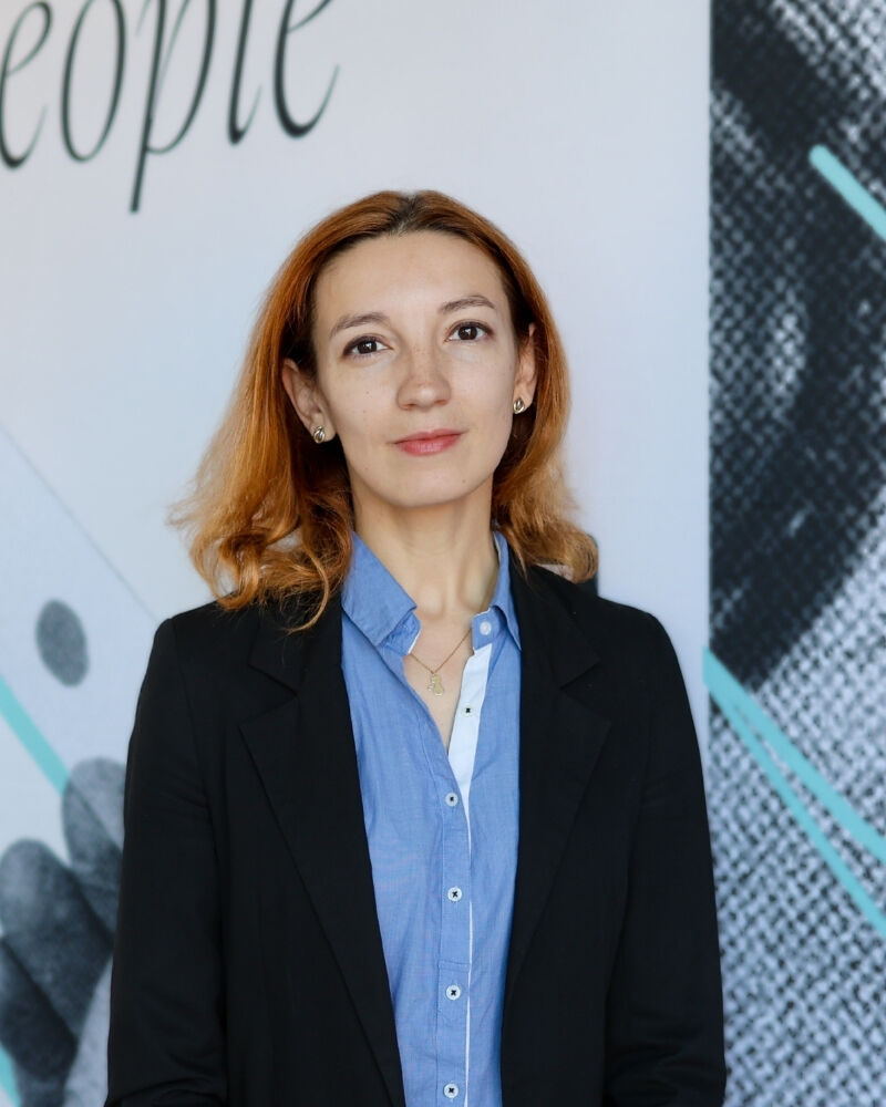
Dr. Anastasiia Lysak
Anastasiia completed her bachelor’s and master’s studies in physics at the National Technical University of Ukraine “Igor Sikorsky Kyiv Polytechnic Institute” between 2011 and 2017, followed by a second master’s degree at the University of Wrocław (Stefan Banach Scholarship). At the Institute of Physics of the Polish Academy of Sciences, she carried out her PhD project between 2020 and 2025, devoted to the growth and characterization of superlattices based on ZnO and CdO layers using PA-MBE, both undoped and in situ europium-doped.
She worked at the Molecular Beam Epitaxy Laboratory of the Institute of Physics, Polish Academy of Sciences, where she focused on the growth of II–VI semiconductor heterostructures and their comprehensive structural, optical, and electrical characterization, using techniques such as AFM, SEM/EDX/CL, PL, UV-VIS, and Hall effect measurements. She is a co-author of over 20 publications, including 5 as first author, and has presented her work at 12 international conferences. She is currently employed in the Advanced Epitaxial Materials (EpiMat) group at the Łukasiewicz Research Network – PORT, where she works on the MOVPE growth of boron-doped group-III nitride heterostructures as part of a project carried out in collaboration with ams OSRAM.
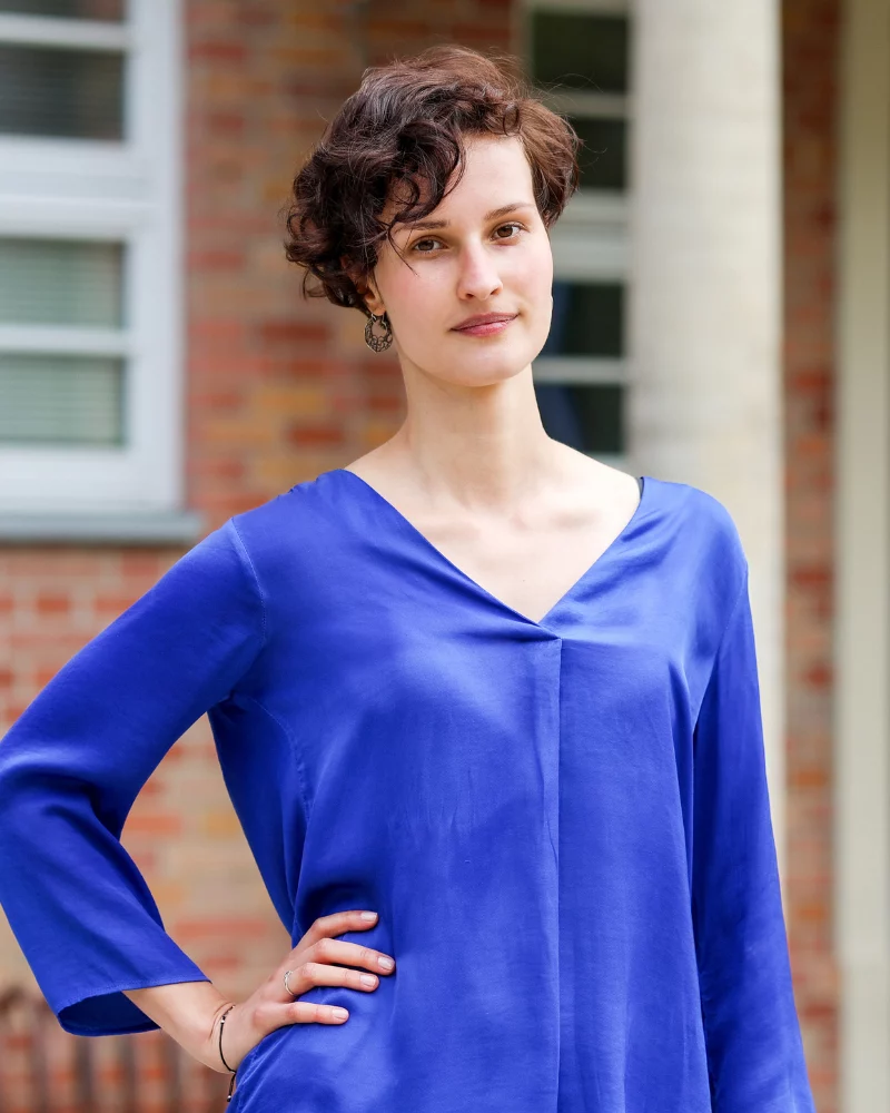
Dr. Dominika Majchrzak
Dominika graduated in Experimental Physics from the University of Wrocław. After earning her master’s degree, she began an industrial PhD at the Institute of Low Temperature and Structural Research, Polish Academy of Sciences (INTiBS PAS) while working in Prof. Detlef Hommel’s research group at the Łukasiewicz Research Network – PORT. Her doctoral work focused on the structural and electrical characterization of semiconductor materials based on gallium nitride.
Dominika’s main task is the structural characterization of semiconductor compounds produced by epitaxial methods, using surface-sensitive techniques such as X-ray photoelectron spectroscopy (XPS) and atomic force microscopy (AFM). She is also involved in the growth of semiconductor samples using molecular beam epitaxy (MBE) and performs Hall effect measurements.
She successfully defended her PhD in March 2023. Since May 2021, she has led a three-year NCN PRELUDIUM 19 project titled “Application of gradient AlGaN contact layers to achieve low-resistivity ohmic contacts in deep-UV emitters.”
She is currently a post-doc in the NCN OPUS 23 project “Hybrid photovoltaic detectors based on a van der Waals/(Al)GaN junction,” supervised by Prof. Robert Kudrawiec.
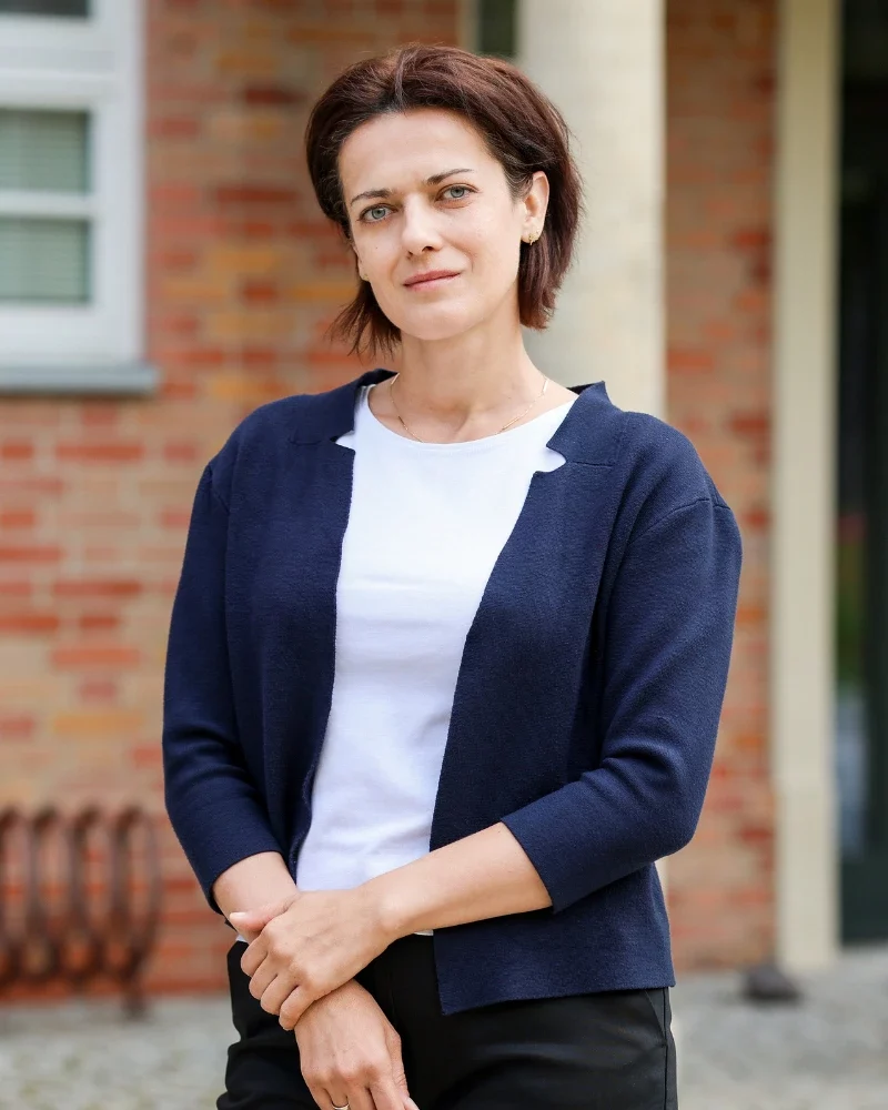
Aneta Mgłosiek
Aneta earned her MSc in Materials Engineering from the AGH University of Science and Technology in Kraków. Her master’s thesis investigated how the physical properties of bottom sediments affect heavy-metal accumulation. In our laboratory, Aneta is responsible for coordinating orders, budget control, documentation, and ensuring the efficient organization of the laboratory’s operations.
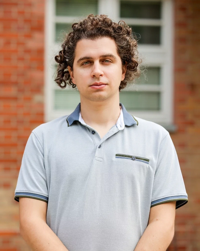
Wojciech Olszewski
Wojciech completed BSc and MSc studies in Experimental Physics at the University of Wrocław. In 2016, during his studies, he began an internship in the epitaxy laboratory at the then EiT+ center (now the Łukasiewicz Research Network – PORT), where he started working with MOVPE. His master’s thesis addressed GaN epitaxy carried out at PORT. He began PhD studies in 2019 and in 2025 submitted his dissertation on GaNAs growth by MOVPE.
He is currently in the third year of an NCN PRELUDIUM project. Within the group, he is responsible for the MOVPE system – growing substrates, new materials, and heterostructures for the team and for his own research.
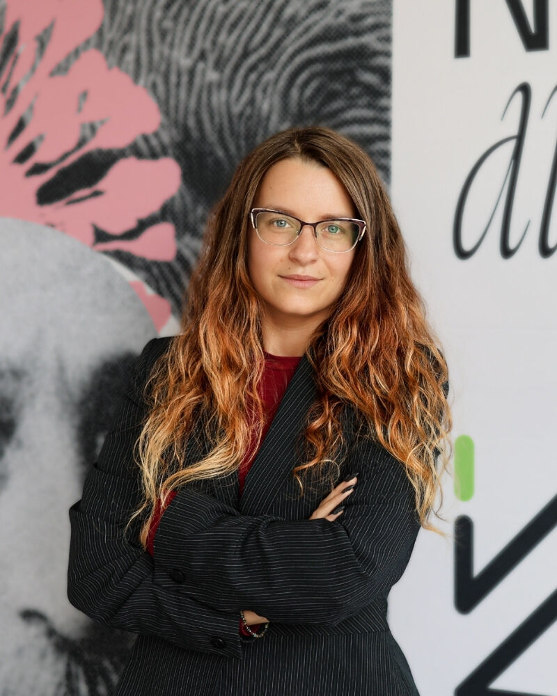
Adrianna Piejko
Adrianna is a materials engineer and PhD student at the Wrocław University of Science and Technology. She completed a BEng in Technical Physics and an MSc in Electronics and Telecommunications. Her doctoral research focuses on two-dimensional materials, in particular transition-metal dichalcogenides (TMDs), analyzing their atomic-scale properties. At the Łukasiewicz Research Network – PORT, she operates metal-deposition systems and participates in semiconductor structure fabrication. Outside of work, she enjoys running, horseback riding, and kitesurfing.
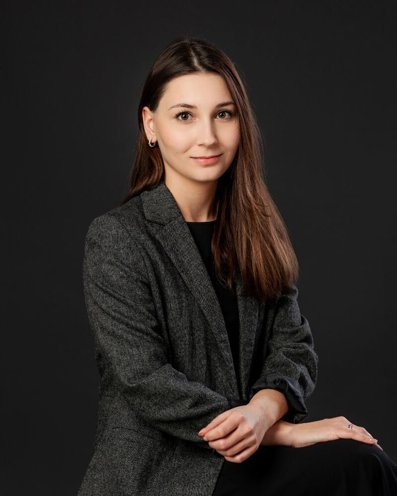
Kamila Nowak
Kamila earned BSc and MSc degrees at the Wrocław University of Science and Technology in Chemical and Process Engineering and Materials Engineering. She is currently pursuing a PhD at WUST in the Department of Nanometrology, Faculty of Electronics, Photonics and Microsystems. The subject of her doctoral research involves novel diluted magnetic semiconductors (DMS) based on group-III nitride materials (GaN, AlGaN).
She specializes in the epitaxial growth of these materials using plasma-assisted molecular beam epitaxy (PA-MBE), as well as in comprehensive structural and surface characterization of semiconductor materials.
Outside science, she enjoys hiking, cycling, and running.

Izabella Danielska
The description of the scientist is in preparation.

Magdalena Wietrzyńska
The description of the scientist is in preparation.

Daniel Gębusia
The description of the scientist is in preparation.