Warsaw University of Technology
Researches
Our group has recently published an article titled “Mode Sensitivity Exploration of Silica–Titania Waveguide for Refractive Index Sensing Applications” in the journal Sensors (MDPI). The article consists of two parts. In the first part, an experimental demonstration of an optical platform based on a silica–titania material is presented. The results were obtained by the team led by Prof. P. Karasiński from the Silesian University of Technology.
In the second part of the article, numerical investigations of a ring resonator structure were carried out by Muhammad Ali Butt, PhD at the Warsaw University of Technology. The sensing device in the form of a ring resonator was modeled using the two-dimensional finite element method (2D-FEM) for refractive index detection applications. A sensitivity of 230 nm/RIU was achieved, a figure of merit (FOM) of 418.2 RIU⁻¹, and a Q-factor of 2247.5 with optimized geometric parameters.

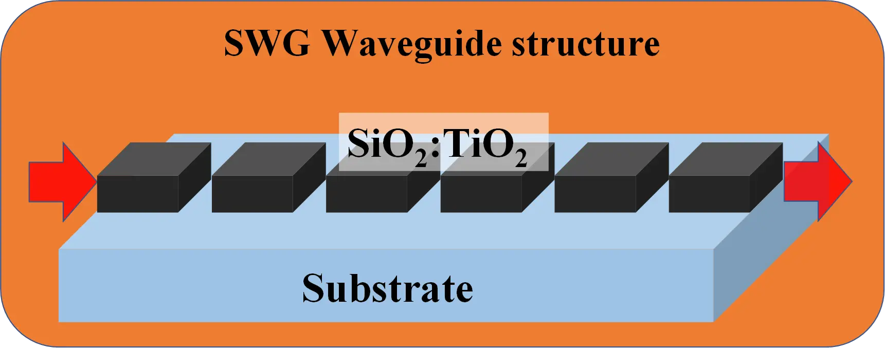
Subwavelength gratings (SWG) are a key element in creating high-performance integrated photonic devices, such as low-loss fiber-to-chip couplers, selective filters, modulators, sensors, and ultra-broadband waveguide couplers. The cross-section of an SWG waveguide corresponds to a rib waveguide, but includes a periodic refractive-index modulation along the propagation direction.
Due to the subwavelength periodicity of the grating, specific wavelength bands can propagate as Bloch waveguide modes. An SWG waveguide with a given grating period or duty cycle (denoted as DC) can be tuned for transmission within a desired wavelength band. These waveguides are particularly attractive because they allow modification of the effective refractive index of the guided mode and its dispersion characteristics.
Our group has published an article on the SWG waveguide structure for filtering and sensing applications in the International Journal of Molecular Sciences. The designed SWG waveguide functioning as an NIR stopband filter (SWG waveguide NIR-stopband filter) achieves an extinction ratio (ER) above 40 dB and a 3 dB bandwidth of 110 nm with optimized parameters.
The SWG–FP waveguide structure proposed in this work serves as a refractive-index sensor, achieving a sensitivity of ~120 nm/RIU by reducing the waveguide width. This sensitivity can be further increased by reducing the waveguide height.
We believe that this work is significant for the development of low-cost integrated photonic devices based on the silica–titania platform developed using the sol-gel dip-coating method.
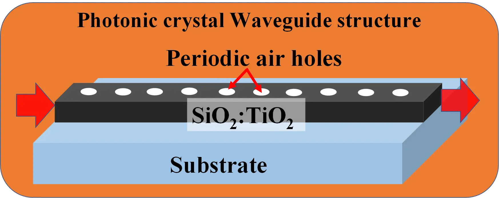
Our group has published an article on a one-dimensional photonic crystal (1D Photonic Crystal, PhC) waveguide based on the silica–titania platform for filtering and sensing applications in Optics Express.
Photonic crystals (PhCs), proposed by Yablonovitch and John, have attracted tremendous interest due to their extraordinary electromagnetic (EM) properties and potential applications in optoelectronics. Photonic bandgaps (PBGs) can be achieved in PhC structures through Bragg scattering in a periodic dielectric structure, in a manner analogous to electronic bandgaps in semiconductors.
This work is the result of collaboration among research partners from:
- Warsaw University of Technology,
- Silesian University of Technology,
- Łukasiewicz Research Network – PORT Polish Center for Technology Development,
- Wrocław University of Science and Technology.
We are currently investigating the possibility of realizing a reverse-rib waveguide structure on the silica–titania platform using wet chemical etching, as shown in the figure. This structure can be fabricated by etching the glass substrate using HF acid, followed by deposition of a high-refractive-index layer (silica–titania or a high-index polymer) via dip-coating.
As a result, light guiding can be achieved in this structure, enabling a low-cost waveguide fabrication technology. Numerical analysis is performed in COMSOL Multiphysics to estimate the fundamental mode. We believe that this waveguide structure may be a highly cost-effective solution and a strong candidate for on-chip optical communication applications.

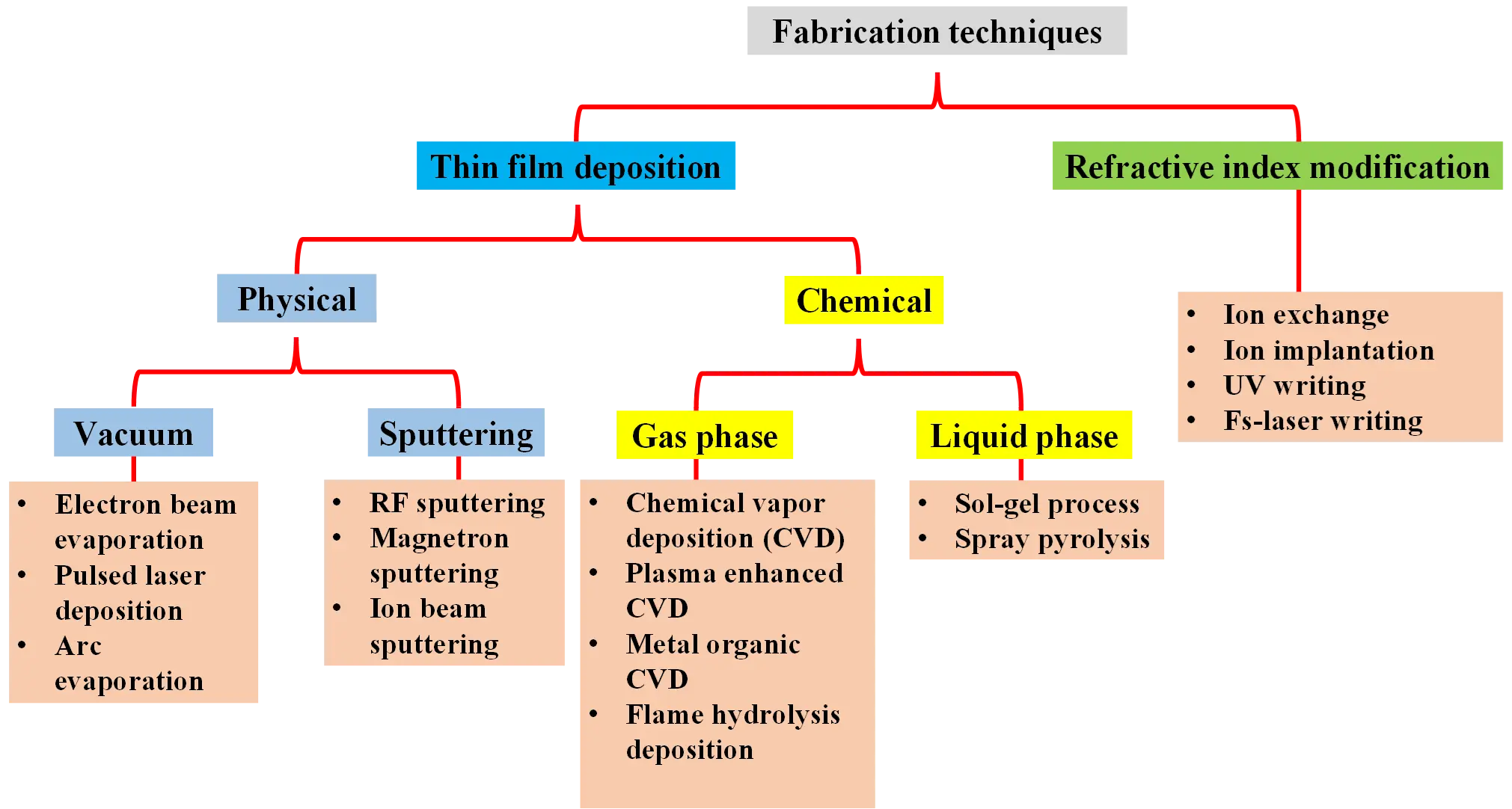
Over the past several decades, a variety of methods for optical thin films have been developed, enabling advances in integrated optics. Our group has published two modern review papers on thin-film deposition techniques. These articles present various approaches to implementing thin-film optical waveguides, including chemical, physical, and refractive-index modification techniques. The figure shows an overview of the most commonly used techniques for fabricating glass optical waveguides.
The latest advances in these fabrication techniques are also discussed. Most developed thin-film fabrication techniques offer high performance; however, they are expensive and require advanced equipment. Researchers’ primary interest focuses on developing simple and cost-effective methods that enable mass production of optical thin films and, consequently, accelerate the commercialization of waveguide technology.
Our research group focuses on developing a silica–titania waveguide platform fabricated using the sol-gel dip-coating method, as well as implementing passive and active optical elements using wet etching. We are also investigating the feasibility of applying nanoimprint lithography (NIL) to pattern these layers to make the fabrication process more efficient and economical.
The latest achievements related to this platform have been discussed. We believe that the silica–titania waveguide technology developed using the sol-gel dip-coating method is highly attractive and cost-effective, and therefore has strong commercialization potential in applications such as sensing and optical interconnects.