
For years, scintillator research has been one of the key areas of work pursued by the Photonic Materials Research Group at Łukasiewicz – PORT. The scientists are developing, among other things, perovskite materials that could offer a more affordable alternative to conventional scintillator crystals. They are also currently exploring the potential of scintillators that emit light in the near-infrared range.
X-rays and gamma rays are invisible to the naked eye. To detect them and protect ourselves from their effects, we need a material that converts their energy into light. This is how a scintillator works.
“A scintillator can be compared to an LED. When an electric current is applied, the LED lights up. Scintillation works in a similar way: ionizing radiation excites the material, which then emits light that can be detected,” explains Dr. Michał Makowski of the Photonic Materials Research Group.
Scintillators are used in computed tomography and positron emission tomography (PET), as well as in radiation detection, high-energy physics, space technologies, and security systems. They make it possible to detect ionizing radiation, which can be harmful to humans at high doses.
A More Affordable Alternative to Conventional Materials
Producing high-quality inorganic scintillators typically requires expensive equipment and advanced manufacturing processes. This contributes to the cost of the crystals used in diagnostic devices such as PET scanners. Perovskites are one possible alternative. They can be produced using simpler methods, including solution-based synthesis.
“Perovskites offer the potential to significantly reduce the cost of synthesizing scintillator materials,” explains Dr. Michał Makowski.
Their large-scale use could eventually lower detector manufacturing costs and, indirectly, make some medical imaging procedures more accessible. Before this becomes possible, however, scientists must improve the durability, stability, and reproducibility of these materials.
How Can Scintillator Performance Be Improved?
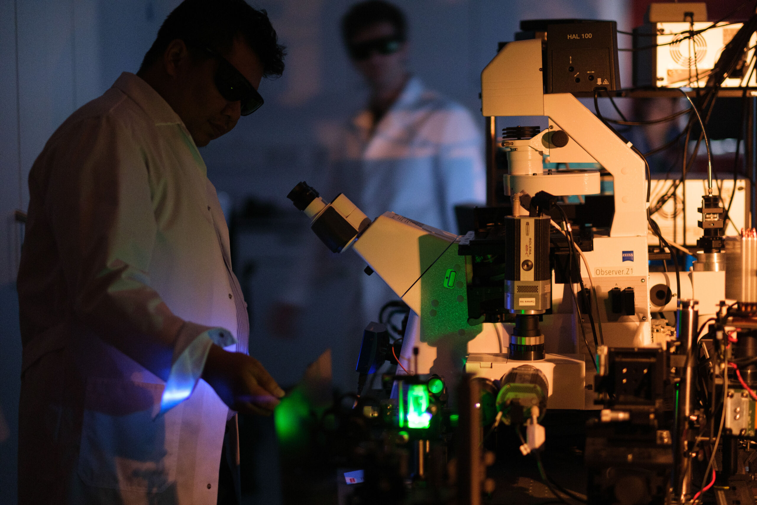
In their day-to-day work, researchers at Łukasiewicz – PORT analyze key scintillator parameters, including light yield and response time. They modify the composition and structure of scintillator materials and investigate how the surrounding environment affects light emission, using approaches such as nanophotonics.
A scintillator can be coupled with specially designed nanostructures that interact with the light it emits. When properly matched, these structures can accelerate emission, increase the intensity of the optical signal leaving the sample, or significantly alter the properties of the emitted light. One of the phenomena studied by the team is the Purcell effect. It occurs when a carefully engineered electromagnetic environment enables an emitter to release its energy as light more quickly and efficiently.
The most important scintillator properties depend on the intended application. Some devices require a very short response time, while others prioritize high light yield, compact size, resistance to environmental conditions, or low cost. Researchers therefore tailor the material’s properties to the needs of each specific application.
Moving Toward the Near-Infrared
Most well-established scintillators emit visible light. The team at Łukasiewicz – PORT is now investigating the possibility of shifting scintillator emission toward the near-infrared range.
In a bulk material, light must travel from the point where it is generated to the photodetector. Along the way, it may be absorbed or scattered by nanocrystals, pores, and interfaces between the components of the composite. These effects are generally less pronounced at longer wavelengths. Near-infrared photons may therefore travel more easily through thick and nonuniform materials.
“We are moving toward the near-infrared range so that we can detect lower-intensity signals. We want our measurement systems to be as resistant as possible to different types of background noise,” says Dr. Michał Makowski.
This is particularly important when detecting weak signals. If the detector receives a large amount of light, minor interference has little effect on the result. When only a small number of photons are detected, however, distinguishing the actual signal from background noise becomes much more difficult.
“Another potential advantage of infrared emission is the theoretical possibility of maximizing the amount of light emitted,” Dr. Makowski adds. “However, this depends on more factors than the wavelength of the emitted radiation alone.”
A Simulation-Based Roadmap
In the article Tuning Light–Matter Interaction of Near-Infrared Nanoplasmonic Scintillators, published in Scientific Reports, Dr. Michał Makowski, Dr. Dominik Kowal, and Dr. Muhammad Danang Birowosuto presented a theoretical model of the interaction between near-infrared scintillators and plasmonic structures.
Using high-precision computer simulations and a quantum-optical model, they studied different types of emitters and nanostructures. They identified the materials, geometries, and parameters that may lead to faster emission or strong light–matter coupling.
“Simulations allow us to identify solutions worth testing in the laboratory without first having to produce numerous costly samples,” explains Michał Makowski.
The publication therefore provides a roadmap for future experiments on near-infrared nanophotonic scintillators. It is part of the group’s broader research into more affordable scintillator materials, improved scintillator performance, and more effective detection of weak radiation signals.