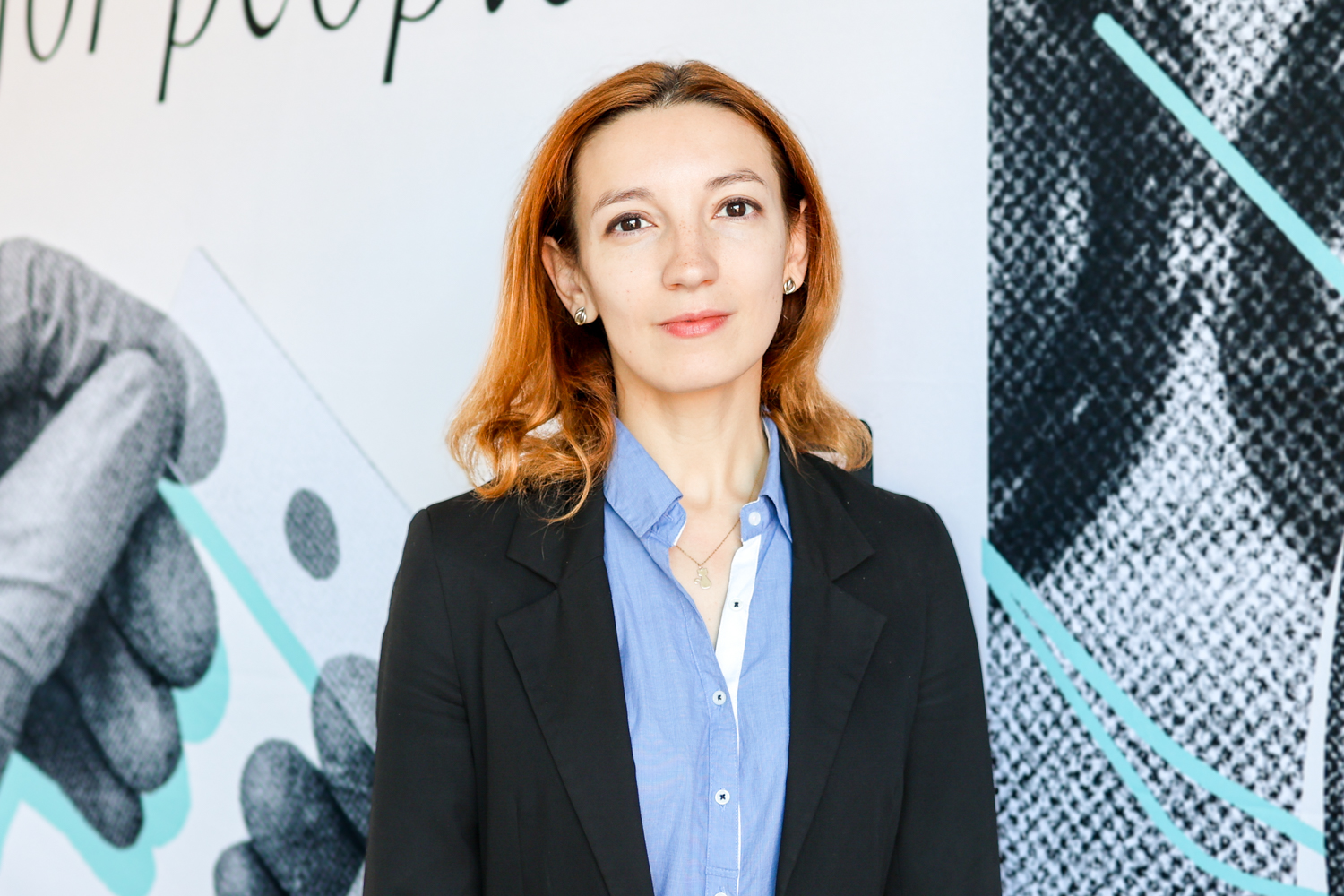
Dr. Anastasiia Lysak will spend three months at Pohang University of Science and Technology (POSTECH) in South Korea. With funding from the National Science Centre’s MINIATURA program, she will advance her research on integrating advanced materials used in semiconductor technologies.
Dr. Anastasiia Lysak works in the Advanced Semiconductor Epitaxy Research Group at Łukasiewicz – PORT, led by Prof. Detlef Hommel. Her research focuses on the growth of group III nitride heterostructures using MOVPE, a technique that enables the controlled fabrication of high-quality semiconductor layers.
She already has experience in this field: her PhD research at the Institute of Physics of the Polish Academy of Sciences focused on the growth and characterization of semiconductor structures. She now plans to expand her research into a new area: integrating two-dimensional materials with nitride semiconductors.
How to Combine a 2D Material with a Semiconductor
Dr. Anastasiia Lysak’s project focuses on combining h-BN (hexagonal boron nitride) with GaN (gallium nitride). GaN is a semiconductor used, among other applications, in optoelectronics, while h-BN is a layered two-dimensional material with unique physical properties.
The challenge is to combine the two materials in a way that produces a stable layer with the desired properties. “We need to identify the right growth conditions so that the h-BN layer is of high quality and forms a suitable interface with GaN. We also want to understand the processes taking place at the boundary between the 2D and 3D materials,” explains Dr. Anastasiia Lysak.
The researcher aims to develop a controlled process for growing h-BN directly on GaN. Currently, h-BN can be integrated with GaN using methods such as layer transfer. The ability to fabricate the entire structure in a single MOVPE process could, in the future, improve the quality and performance of semiconductor and optoelectronic devices, including DUV LEDs, photodetectors, and transistors.
Learning from Experts in h-BN and GaN
The choice of South Korea was no coincidence. POSTECH is home to Prof. Jong Kyu Kim’s team, one of the leading research groups working on h-BN and its growth on GaN.
“I chose this group because it has extensive experience in this field and a strong publication record on these materials. I want to broaden my knowledge of both their growth and characterization,” says Dr. Lysak.
During her three-month stay, she will work on growing h-BN layers on GaN, study their properties, and analyze the processes occurring at the interface between the two materials. An important part of the internship will also be learning methods for characterizing extremely thin layers and using research infrastructure that makes it possible to move from material growth to the fabrication of prototype devices.
The research internship in South Korea will provide Dr. Lysak with practical know-how that she will be able to apply to further developing the h-BN/GaN process in the laboratories of the Wrocław-based institute. “At Łukasiewicz – PORT, we have the capabilities to prepare such structures, so we will be able to continue developing this research direction step by step,” says Dr. Lysak.
In the longer term, the research could provide a foundation for larger projects and collaboration with other centers working on semiconductor technologies.