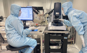
Clean Room laboratory
Clean Room Laboratory is located in an ISO 5 and ISO 6 class room.
The main methods developed and deployed at the laboratory are optical and electron lithography, production of metallic and dielectric layers, and wet and plasma etching. Our ambition is also to develop technology in manufacturing thin films using atomic layer deposition. Moreover, the laboratory has full capacity to analyze and validate structures and microcomponents.
Clean Room area
The Clean Room Laboratory is located in rooms with ISO 5 and ISO 6 cleanliness classes according to ISO 14644 standard. We have clean rooms with a total area of > 600 m2. In this type of laboratory, we have constant monitoring of parameters such as temperature and humidity. Periodic cleanliness measurements confirm the cleanliness class. The amount of dust or other micro-particles is kept constantly low. Additionally, the rooms designed for lithography are equipped with special lighting systems that minimize the amount of light that could interfere with the photolithography process.
Experimental Techniques
The main techniques developed and implemented in the laboratory are photolithography, optical maskless lithography, metal and dielectric layers deposition (magnetron sputtering, e-beam evaporation, PECVD) as well as wet and plasma etching (ICP-RIE). Our ambition is also to develop competence in the production of thin layers by the atomic layer deposition (ALD) method and the printing of high resolution metal lines for integrated electronics. The laboratory has full capability for the analysis and validation of fabricated structures and layers, through precise microscopy, spectroscopic ellipsometry and two profilometers – contact and optical.
Topics and Activities
We offer commercial services to companies and research institutions that require advanced microfabrication techniques and the characterization of micro/nanostructures and layers. We welcome research contracts and joint project proposals. Our team collaborates with various research groups, both within PORT and from other institutions, in topics such as III-V semiconductor-based optoelectronics, sol-gel-derived silica-titania photonic circuits, and advanced materials like perovskites and artificial opals. Our primary expertise lies in the fabrication of planar photonic components using lithographic methods. Currently, our main research focus is the development of biosensors based on photonic integrated circuits (PICs).
The Clean Room Laboratory is located in rooms with ISO 5 and ISO 6 cleanliness classes according to ISO 14644 standard. We have clean rooms with a total area of > 600 m2. In this type of laboratory, we have constant monitoring of parameters such as temperature and humidity. Periodic cleanliness measurements confirm the cleanliness class. The amount of dust or other micro-particles is kept constantly low. Additionally, the rooms designed for lithography are equipped with special lighting systems that minimize the amount of light that could interfere with the photolithography process.
Patterning Methods:
- Photolithography (resolution about 1 µm)
- Maskless optical lithography (resolution about 1 µm)
- Printing of conductive tracks (diameter from 5 µm, any shapes)
Thin Film Deposition:
- Deposition of dielectric and conductive layers (evaporation, magnetron sputtering, PECVD)
- Application of layers using liquid method (spin-coating, dip-coating)
- Atomic Layer Deposition – ALD
Etching:
- Wet etching of different materials (semiconductors, oxides, nitrides, etc.)
- Reactive plasma etching of materials based on silicon and semiconductor compounds (ICP/RIE)
Additional Processes:
- Rapid thermal processing (RTP)
- Annealing (furnace, precise hot plates)
- Wet and plasma cleaning
Characterization:
- Contact profilometry
- Optical profilometry
- Optical microscopy
- Spectroscopic ellipsometry
Lithography:
- SÜSS MicroTec Mask Aligner MA8/BA8
- Heidelberg Instruments µMLA Tabletop Maskless Aligner
- Spin coaters (SÜSS RCD8, Laurell)
Vacuum deposition/sputtering:
- Moorfield MiniLab 060 (e-beam evaporation)
- Moorfield MiniLab 080 (magnetron sputtering)
Chemical vapor deposition:
- Sentech SI 500 208 (PECVD, layers: SiO2, Si3N4)
Plasma etching and cleaning:
- Sentech SI 500 206 (ICP-RIE, gases: Ar, O2, SF6, CF4, CHF3, C4F8)
- Sentech SI 500 207 (ICP-RIE, gases: Ar, O2, SF6, CF4, SiCl4, BCl3, Cl2)
- TePla GIGAbatch 310M (microwave plasma, gases: O2, CF4)
Annealing:
- RTP AS-One 150 (rapid thermal annealing)
- SÜSS HP8 Hot plate (x3)
Conductive tracks creation:
- XTPL Delta Printing System
Characterization and measurements:
- Inspection microscopes: Leica DM 4000, DM 8000, Keyence VHX-7000
- Bruker DektakXT (contact profilometer)
- Bruker ContourGT (optical profilometer)
- Sentech SE850 DUV (spectroscopic ellipsometer)
2024
- Łukasz Duda, Krzysztof Rola, Michał Łukomski, Andrzej Gawlik, Jacek Olszewski, Maciej Czajkowski, Joanna Cybińska, Małgorzata Guzik,
“Fabrication of luminescent disc-shaped microstructures via wet-chemical etching of hybrid sol–gel layers for potential photonic applications”,
Journal of Materials Science (2024). DOI 10.1007/s10853-024-10059-y - Krzysztof Rola, Łukasz Duda, Sandeep Gorantla, Krzysztof Czyż, Małgorzata Guzik, Joanna Cybińska,
“Focused Electron Beam Micro- and Nanopatterning of Thin Films Derived from Sol-Gels Based on TiO2 Precursors for Planar Photonics”,
ACS Applied Nano Materials, Volume 7, Issue 8, pp. 8692–8702 (2024), DOI 10.1021/acsanm.4c00060 - Daria Hlushchenko, Jacek Olszewski, Tadeusz Martynkien, Michał Łukomski, Karolina Gemza, Pawel Karasiński, Magdalena Zięba, Tomasz Baraniecki, Łukasz Duda, Alicja Bachmatiuk, Małgorzata Guzik, Robert Kudrawiec,
“Waveguide-Coupled Light Photodetector Based on Two-Dimensional Molybdenum Disulfide”,
ACS Applied Materials & Interfaces Volume 16, Issue 22, pp. 28874-28885 (2024), DOI 10.1021/acsami.4c04854
2022
- Łukasz Duda, Maciej Czajkowski, Paweł Karasiński, Cuma Tyszkiewicz, Magdalena Zięba, Małgorzata Guzik, Alicja Bachmatiuk,
“Towards facile fabrication of photonics components from inorganic and hybrid sol-gel films. Preparation and optical properties characterization”,
Ceramics International, Volume 48, Issue 20, pp. 29676-29685 (2022), DOI 10.1016/j.ceramint.2022.06.225. - Paweł Karasiński, Magdalena Zięba, Ewa Gondek, Jacek Nizioł, Sandeep Gorantla, Krzysztof Rola, Alicja Bachmatiuk, Cuma Tyszkiewicz,
“Sol-Gel Derived Silica-Titania Waveguide Films for Applications in Evanescent Wave Sensors—Comprehensive Study”,
Materials, Volume 15, Issue 21, article number 7641 (2022), DOI 10.3390/ma15217641 - Muhammad A. Butt, Cuma Tyszkiewicz, Paweł Karasiński, Magdalena Zięba, Daria Hlushchenko, Tomasz Baraniecki, Andrzej Kaźmierczak, Ryszard Piramidowicz, Małgorzata Guzik, Alicja Bachmatiuk,
“Development of a low-cost silica-titania optical platform for integrated photonics applications,”
Optics Express, Volume 30, pp. 23678-23694 (2022), DOI 10.1364/OE.460318
2021
- Krzysztof Rola, Adrian Zając, Andrea Szpecht, Dominik Kowal, Joanna Cybińska, Marcin Śmiglak, Katarzyna Komorowska,
“Interaction of electron beam with ionic liquids and its application for micropatterning”,
European Polymer Journal, Volume 156, article number 110615 (2021), DOI 10.1016/j.eurpolymj.2021.110615 - Dominik Kowal, Krzysztof Rola, Joanna Cybińska, Marcin Skoreński, Adrian Zając, Andrea Szpecht, Marcin Śmiglak, Sławomir Drobczyński, Karolina Ciesiołkiewicz, Katarzyna Komorowska,
“Fluorescent ionic liquid micro reservoirs fabricated by dual-step E-beam patterning”,
Materials Research Bulletin, Volume 142, article number 111434 (2021), DOI 10.1016/j.materresbull.2021.111434
2019
- Krzysztof Rola, Adrian Zając, Maciej Czajkowski, Andrea Szpecht, Maria Zdończyk, Marcin Śmiglak, Joanna Cybińska, Katarzyna Komorowska,
“Ionic liquids for active photonics components fabrication”,
Optical Materials, Volume 89, pp. 106-111 (2019), DOI 10.1016/j.optmat.2019.01.003 - Krzysztof Rola, Adrian Zając, Maciej Czajkowski, Marta Fiedot-Toboła, Andrea Szpecht, Joanna Cybińska, Marcin Śmiglak, Katarzyna Komorowska,
“Electron Beam Patterning of Polymerizable Ionic Liquid Films for Application in Photonics”,
Langmuir, Volume 35, Issue 37, pp. 11968-11978 (2019), DOI 10.1021/acs.langmuir.9b00759 - Adrian Zając, Andrea Szpecht, Dawid Zieliński, Krzysztof Rola, Jakub Hoppe, Katarzyna Komorowska, Marcin Śmiglak,
“Synthesis and characterization of potentially polymerizable amine-derived ionic liquids bearing 4-vinylbenzyl group”,
Journal of Molecular Liquids, Volume 283, pp. 427-439 (2019), DOI 10.1016/j.molliq.2019.03.061 - Krzysztof Rola, Adrian Zając, Joanna Cybińska, Marcin Śmiglak, Katarzyna Komorowska,
“Polymerizable ionic liquids for microstructures fabrication”,
Proceedings of SPIE – The International Society for Optical Engineering, Volume 10915, Article number 109151E, Organic Photonic Materials and Devices XXI 2019, DOI 10.1117/12.2509680
2018
- Krzysztof Rola, Adrian Zając, Maciej Czajkowski, Joanna Cybińska, Tadeusz Martynkien, Marcin Śmiglak, Katarzyna Komorowska,
“Ionic liquids – A novel material for planar photonics”,
Nanotechnology, Vol. 29, article number 475202 (2018), DOI 10.1088/1361-6528/aae01e
On-going projects:
- “Application of photonic crystals in originality protections“ (project acronym: Anti-Copy)
Project financed by the National Centre for Research and Development under the “Lider XII” program
Total cost: 1 496 487,50 PLN
Duration: 01/03/2022 – 01/03/2025
Principal Investigator: Maciej Czajkowski, Ph.D.
Completed projects:
- “Hybrid sensor platforms of integrated photonic systems based on ceramic and polymer materials” (project acronym: HYPHa)
Project financed by the European Union from the European Regional Development Fund under the TEAM-NET program of the Foundation for Polish Science
Total cost: 13 208 000,00 PLN
Total cost (on the side of Łukasiewicz – PORT): 3 499 250,00 PLN
Duration: 01/10/2019 – 30/09/2023Project realized in a consortium:
Łukasiewicz Research Network – PORT Polish Center for Technology Development – Consortium Leader
Wrocław University of Science and Technology
Silesian University of Technology
Warsaw University of Technology
Principal Investigator: Alicja Bachmatiuk, D.Sc., Ph.D., Eng.
Group Leader (on the side of Łukasiewicz – PORT): Małgorzata Guzik, D.Sc., Ph.D. - “Technology development for the production of passive anti-icing systems based on innovative superhydrophobic epoxy nanocomposite coatings” (project acronym: ICE)
Project financed by the National Centre for Research and Development under the “Lider IX” program
Total cost: 1 199 825,00 PLN
Duration: 01/01/2019 – 31/12/2021
Principal Investigator: Jacek Marczak, Ph.D. - “Fabrication and optimization of photonic components by electron and ion beam induced polymerization of ionic liquid monomers” (project acronym: FACILE)
Project financed by the National Science Centre, Poland under the „OPUS 10” program
Total cost: 1 326 700,00 PLN
Total cost (on the side of Łukasiewicz – PORT): 624 200,00 PLN
Duration: 24/10/2016 – 23/04/2020
Project realized in a consortium:
Wrocław Research Centre EIT+ – Consortium Leader
Adam Mickiewicz University Foundation
Principal Investigator: Katarzyna Komorowska, Ph.D., Eng.
Request a quotation:
zapytania@port.lukasiewicz.gov.pl
Laboratory Manager:
Krzysztof Rola, Ph.D.
krzysztof.rola@port.lukasiewicz.gov.pl